HW Open Source 6.5 Digital Voltage Meter (Part1: Schematic and working principle)
HW
Open Source 6.5 Digital Voltage Meter (Part1: Schematic and working principle)
This is an open HW project, the target is
to build up a low cost high precise voltage meter with 6.5 digital resolution,
and ±50V input range. It has the capability to controlled by the upper level
control system and has a VFD display that can make it work independently.
This series of articles will be divided
into at least 3 parts:
Part1: Schematic and working principle
introduction.
Part2: HW Debugging and bug fix.
Part3: Calibration and performance test.
Part4: Temperature coefficient compensation
(not sure whether it works or not)
DIY Disclaimer
In this DIY project you may need to
use high voltage, electric soldering iron, etc. unfamiliarity with the tools
and process can be dangerous. This project should be viewed as entertainment
only. The author will not be held responsible for any injury due to the misuse
or misunderstanding of this DIY project. It’s purely “at your own risk”. If you
are at all uncomfortable or inexperienced working on projects yourself
(especially projects involving dangerous tools), please reconsider doing it by yourself.
It is very possible on any DIY to damage your property, create a hazardous
condition, or harm or even kill yourself or others. I am not at all
responsible for the actions you take after you have read this article.
DIY Background:
I bought 2 ADS1256 modules planned for my LCR
meter project, before I got all the material for my LCR meter project, I got several
VFD displays occasionally, then I put these 2 things together and found it
works quite well, you can see the prototype here:
https://aduecho.blogspot.com/2021/03/build-low-cost-65-digital-voltage-meter.html
This acritical will focus on the PCB version, which named Version 1.0.
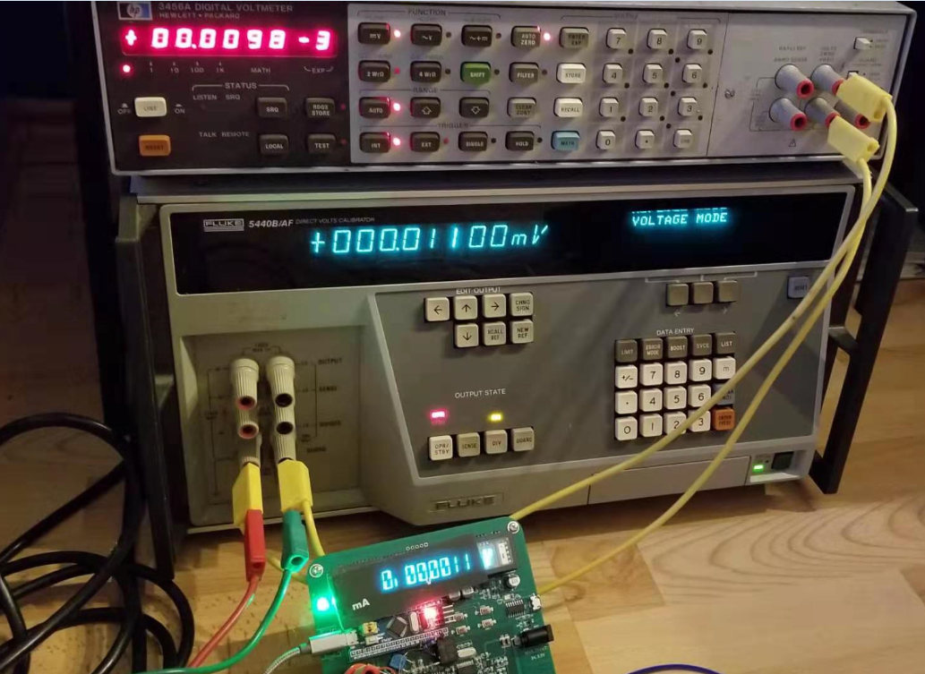
Base Range test result:
After some HW bug fixed, here are some pictures for the base range(±2.2V) testing, for the detail it will be descripted in Part B and Part C.


Schematic introduction:
1.1 ADC part
The core part is ADS1256, it’s a Very Low Noise, 24-Bit
Analog-to-Digital Converter.
Can provide up to 23 Bits Noise-Free Resolution. It integrates
a 1-64x low noise PGA, which helps for low level voltage measurement.
The whole system power by 5V, in order to accept true
bipolar voltage input we need to set the VCM to 2.5v, then the span at ADC
input port is ±2.5V, considering we need to give some space to the input amplifier,
thus the max linearity input range for ADC is ±2.2V(referring VCM).
The ADS1256 has an internal 2x amplifier for the reference,
in order to use the full range of the ADC, we need to set the Vref to 1.25V.
The input channel 2&3 are connected to VREF directly,
used for ADC gain performance testing. And channel 4&5 short circuit, for
ADC noise evaluation.


1.2 Voltage Reference
Considering cost and performance, it’s not easy to find a suitable
1.25v voltage reference for ADS1256. We need to find a low noise and low drift
reference to match with ADS1256’s performance. And the minimal input voltage
for the reference IC should be less than 5V, finally chose REF5025, here it’s
the key parameter for this IC, and seems VSSOP has a better performance compare
to SOIC-8 package, so here chose the VSSOP package, it’s a bit difficult for
hand soldering.


Resistor R1 & R2 working as voltage divider,
the resistor using here should have the same or similar temperature coefficient,
in order to reduce the temperature’s influence.
And U5 OPA350 used to buffer the 1.25V, and
it can drive huge capacitor, provide the peak current which is needed when
ADS1256 running at high ODR mode. But the weakness point is OPA350’s 1/f noise
is too high, which is not mentioned in the datasheet. It seems there is no
better choice, since the evaluation board for ADS1256 from TI is also using
OPA350 as buffer, maybe it's a compromise.

1.3 Analog input circuit and self-calibration circuit
J1 and J2 are the
input terminals. J2 connect to the VCM directly. J1 connected to the DVM_IN+ via
a reed relay. The reed relay used to switch the analog frontend to self-calibration
circuit and input terminal. The purpose of using reed relays here is to reduce
the EMF voltage, but during debugging it turned out using reed relay (HE721C0500)
here is totally wrong.
The DVM+ signal can be
routing to RNG_L or RNG_H via a low leakage SPDT analog switch U6.
R9/R10/L4/C19/C20 forms
a low pass filter for the low range, with a BW 100Hz. This filter refers to HP34401A’s
low range filter.
For the low range the
voltage divider is not used, in order to maintenance a high input impedance. And
the low range’s range is ±2.2V.
For the RNG_H, the input
impedance is 10M, RNG10’s gain is ~1/5, RNG20’s gain is ~1/10, and RNG50’s gain
is ~0.43/10. The range switching is done by a low leakage 4:1 analog switch.
The input voltage id
buffered by AD8628, it’s a RRIO amplifier, with a typical 50pA offset current,
and 0.5uVpp low frequency noise. What’s more, it’s available in JCL SMT library.
U3 is a low cost dual
RRIO amplifier, one channel is used to buffer the 2.5V from the reference IC,
used as system common mode voltage (VCM). And another channel is working as an
adder, add 1.25V reference and 2.5V VCM together used for self-calibration.
U2’s part B can route
the DVM+ to VCM or 1.25V Vref for system offset/gain calibration for each
range. The connector “CAL” is used for outside calibration.
The voltage divider’s
absolute accuracy is not so important, theoretically the ratio can be
calculated during calibration.
Notice: there is a
fatal error in the high range voltage divider. I will descript it in Part B.


2.1 VFD driver
circuit
The VFD (SAMSUNG
HCS-12SS59T) need a relative high voltage (Vdis=33V) to provide electric field
for electron acceleration, here using the low cost MC34063 to build a boost circuit.
Q1 used as power supply switch, since the datasheet request the display voltage
must turn on after the filament voltage is given and turn off before the filament
voltage is off. R26, C25, C26 are the RC oscillator for the VFD. It needs a
39pf capacitor but in the LC SMT library this value is not available, so use 2 available
values in parallel here.
The VFD connect to the
MCU via SPI interface.

3. MCU circuit
The system using
STM32f103C8t6 blue-pill board as controller. It gives the chance that user can
use the Arduino to control this system as they want.
On the board it offers
a USB to TTL convertor, connect to the USART port of STM32 blue pill board. And
a CAN transceiver is also reserved, maybe I can use it to connect with many
boards in parallel, then making an average of the measuring result in order to
reduce the noise.
R35&R36 used as a voltage divider, connect to the blue pill’s ADC channel, to monitoring the system voltage, and control the display's voltage.

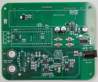
The PCB is 120mm*100mm,
with 4 layers.

You can find the schematic here:
https://drive.google.com/file/d/1PfmhBDpNsJP1FyqyJ5L2pe54IcSiVEGW/view?usp=sharing
and Gerber file here:
https://drive.google.com/file/d/1KaQ4vSXYg2az2gumgiCddYIEk65w-MtM/view?usp=sharing
In the next article I
will introduce the debugging and HW bug fix, as you may notice there are many modifications
in the real PCB board.

评论
发表评论