HW Open Source 6.5 Digital Voltage Meter (Part2: HW Debug and bug fix)
This is an open HW project, the target is to build up a low cost high precise voltage meter with 6.5 digital resolution, and ± 50V input range. It has the capability to be controlled by the upper level control system and has a VFD display that can make it work independently.
This series of articles will be divided into at least 3 parts:
Part 1:
Schematic and working principle introduction.
https://aduecho.blogspot.com/2021/05/hw-open-source-65-digital-voltage-meter.html
Part2: HW debugging and bug fix.
Part 3: Calibration and performance test.
Part4: Temperature coefficient compensation (not sure whether it works or not)
DIY disclaimer
In this DIY project you may need to use high voltage, electric soldering iron, etc. unfamiliarity with the tools and process can be dangerous. This project should be viewed as entertainment only. The author will not be held responsible for any injury due to the misuse or misunderstanding of this DIY project. It's purely “at your own risk”. If you are at all uncomfortable or inexperienced working on projects yourself (especially projects involving dangerous tools), please reconsider doing it by yourself.
It is very possible on any DIY to damage your property, create a hazardous condition, or harm or even kill yourself or others. I am not at all responsible for the actions you take after you have read this article.
1.1 Soldering other components
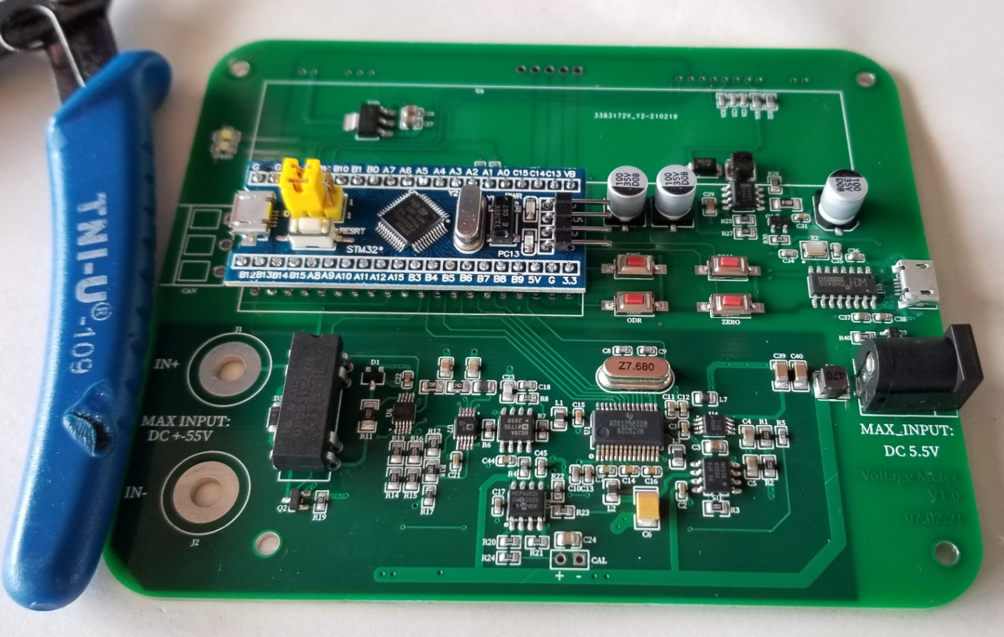
The PCB is manufactured by JLCPCB, and some components already assembled by JLCSMT service if those components available there. Here is the PCBA that I got from JLC, the ADC, voltage reference, analog switches, micro usb connectors are missing, since they are not available in JLCSMT.

Then solder these components manually and clean the PCBA with "WD-40 Specialist Contact Spray", following with alcohol ultrasonically cleaning. Notice: the relay and crystal oscillator may get damage under ultrasonically cleaning, so soldering these parts after cleaning.


Here is the PCBA after cleaning:
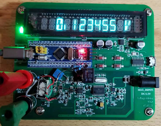
1.2 Board test
After the PCB is completely dry, we can test the board. 1st check all the voltages (3.3v, 5v, 2.5v, 1.25v, 3.75v, 33v) are normal, then we can conduct some system test, mainly focus on the noise, because nobody want to have a voltage meter which always giving you beating numbers.
1.2.1 ADC chip offset test
Set the ADC input channel to channel 4 & 5, ODR = 2.5 Hz, then we can make noise test. The result is sent to the PC by Visual Com Port of STM32, and the data processed by MS excel. The unit in mV. Here captured ~ 6k raw samples, the RMS noise is 0.29uV, peak to peak noise is 2.08uV, seems not bad.


1.2.2 ADC chip gain test
Set the ADC input channel to channel 2 & 3, do the gain noise test. Here captured ~ 12k raw samples, the RMS noise is 0.46uV, peak to peak noise is 4.17uV, seems also not bad.

1.2.3 system noise test


Here select the measurement range to RNG_L (U7 S1 connect with D, U6 D1 connect with S1B), DVM_IN + rout the VCM (by RLY1 and U6 D2_S2A), the logging of the measurement result to PC.
The measurement result is very bad, it's randomly noise at mV level. Then try to locate the noise source step by step.
The 1st suspicious part is the reed relay, take another one and measure the voltage at normal close terminal, it shows ~ 20UV, and it's always jumping, it Should be EMF voltage. Using reed relay here is failure, or at least using this type reed relay is a failure design.

It's almost impossible to find a compatible relay to replace this HE721C0500 relay. Then using an adapter seems the best work around here. Here designed 3 different types of relay adapter, in order to check which is the best (at the end it turned out that, these 3 types of relay's EMF is similar).


While waiting for the adapter PCB, using flying cable to continue others debug.

After replacing the input relay, the system noise is still not good, still at mV level, there is no significant improvement.
Make a plot of the noise, it seems the system starting oscillating. Using an oscilloscope to locate the oscillating point, found the buffer's (ad8628) output is oscillating.
After the ferrite bead L1 has been removed, the oscillating is gone. The reason is clear now: due to the low DC impedance of L1, the operation amplifier is not capable to driver the 10nf (C14) sample capacitor directly, then the system starts to oscillate.

Due to the ADC's impedance is low, it will draw about 12uA current during sampling phase, so the impedance should be as low as possible, but the premise is we need to keep the system stable.
After some test, the minimal value for L1 should be 1ohm, in order to leave some buffer, the ferrite bead L1 and L2 are replaced by 10ohm resistors.
After this, the system noise getting better, but still not perfect, the rms noise is 43.4uV.

Considering the high current consumption during the ADC sampling phase, the noise may cause by the sample hold capacitor C14's value is too small (10nF). Change it to 0.22uf and test again, the noise back to normal: 0.3uV.

Let the system running 1.6 hours, with 14k samples, the noise level is still around 0.3uv, it seems very good, but the problem comes soon.

Measuring a 1.25V reference IC, the value seems always dropping down. The 1.25V reference IC under test is already proved quite stable. This indicate the system's reference is changing.

The board's reference comes from a voltage divider R1 & R2, buffered by U5. R1 & R2 are provide by JLCSMT, they are normal 1% 0805 resistors, the temperature coefficient is unknown, normally it won't better than 250ppm / ° c.

Remove R2, using 2.5v as the board's reference voltage, measuring the 1.25v reference, the noise seems much better now. (the mean / std / max / min value here are already doubled due to the reference doubled)

Seems the drift caused by R1 & R2. Replace them with VISHAY 10ppm / ° c precise resistor.

Test it again, it's getting better but still not as good as w / o voltage divider, and the drifting direction is reversed. Maybe combine these two types of resistors together can eliminate the drift a lot.

The VISHAY resistors package is not compatible with the original package design (0805), in order to make the board looks better, so using 25ppm 0805 resistor replace the R1 & R2. Measure the 1.25v reference for one night (~ 7.7Hours), the drift in first 13mins quite huge, around -100uV, then it is getting stable for short term.

Here is the short term (~ 11mins) test result after it get stable:
The intention to use 1.25V as ADC's reference is to use the full range of ADS1256, when it is using 1.25V reference, the analog input range is ± 2.5V.
When it is using 2.5V reference, then the ADC quantization range is ± 5V. But the electronic maximum analog input range is still ± 2.5V, so one bit of the ADC will be useless.
So, using a good 1.25V reference IC like LTC6655 or LTC6657 would be the best solution, just the price is much higher compare with the REF5025.
Base on the experiments I did in the past: " the reference buffer OPA350 will have negative impact for the noise ", so I take another PCB and modify the circuit, using REF5025's 2.5V output as reference directly.
Here are the changes:
Short R1, R3, U5's Pin2 & 3, remove U5, R2, now the ADC's reference is powered by REF5025 directly.
For the self-calibration circuit, remove U3, short R20-R23. Now the VCM is driven by REF5025 directly. And the self-gain calibration will be using Vref & AGND, in the past it's VCM & (VCM + Vref = 3.75).

Here at right side is the modified version, name it as version B.

Using version B measure the 1.25V reference again, the rms noise is 1.3uV without OPA350, with OPA350 the noise is 0.92uV. This is the opposite of the conclusion I got from the module test before: “ OPA350 have negative impact to the noise performance ”. I'm not sure if this is caused by statistical error, or a device difference or the test environment. Just keep both version and check the performance difference in other tests.

Short summary:
When the input voltage is 0v, the noise is mainly contributing by the ADC, The ADC's rms noise is ~ 0.3uV, quite close to the datasheet's 0.247uV.
When the input voltage close to the reference voltage, the noise is mainly contributing to the voltage reference. Using a low-cost voltage divider to divide the 2.5V reference is not a good idea. If there is a next version, the reference will be replaced by LTC6655-1.25.
The benefit of reference buffer OPA350 is unknown, so in version B the buffer is removed.
2. Fix the bug of voltage divider
The voltage divider has a bug, if input voltage higher than 3V, it will be clamped by the input protection diode D1, also by the ESD protection diodes inside U6.
The same thing happened at U7, for example if the voltage at RNG20 is 5V, then the voltage at RNG10 is already 10V, which is already trigger the internal ESD protection diodes inside U7.
If using relay instead of these analog switches, there won't be so many problems. Using JEFT is also may be a good solution, but the driver circuit is a bit complex, it's not a good workaround on this PCB.
Finally, the modification as below, the input impedance was changed for the RNG20 and RNG50, now the impedance for 2V range is the impedance of AD8628, at Gohm level. Range 10V's impedance is still 10M, RNG20's impedance is 9M, and RNG50's impedance is 8.3M.
In order to reduce the noise caused by the input resistors R13-R16, (Johnson noise + AD8628 input current noise), another relay RLY2 is introduced. It will short R13-R16 in the low range.

Now the board looks ugly, but at least the voltage divider is working now:


Here is the performance comparison, both boards are not calibrated.

Both boards are powered by laptop's USB port, in order to log the measurement data to the PC.
I notice if the board powered by a good USB adapter, the noise will be better, the VFD display jump max 1 digital (1uV) when the input is short. I will find a USB hub which has dedicated power supply and do the test again in calibration paragraph.

评论
发表评论